
CD4051BM/CD4051BC is a single 8-channel analog multiplexer/demultiplexer, CD4052BM/CD4052BC is a dual 4-channel analog multiplexer/demultiplexer, CD4053BM/CD4053BC is a triple 2-channel analog multiplexer/demultiplexer. These analog multiplexers/demultiplexers have low 'ON' impedance and very low 'OFF' leakage currents, and can be controlled by digital signals.
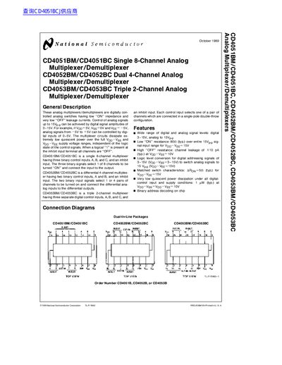
The CD4051BM/CD4051BC is a single 8‑channel analog multiplexer/demultiplexer with three binary control inputs (A, B, C) and an inhibit input. It switches analog signals with low ON resistance and very low OFF leakage, supporting digital control voltages from 3 V to 15 V and analog signal ranges up to ±15 Vpp.
The document includes absolute maximum ratings, DC and AC electrical characteristics, pin‑out diagrams, switching time waveforms, physical dimensions for various package styles, and a life‑support policy notice. It is intended for designers who need detailed performance data for circuit integration.
| Typical ON resistance | 802 Ω (typ.) |
|---|---|
| Typical OFF leakage current | 10 pA (typ.) at Vpp—VEE = 10 V |
| Supply voltage range | 0.5 V to +18 V |
| Input voltage range | –0.5 V to Vpp + 0.5 V |
| Power dissipation (DIP) | 700 mW |
| Power dissipation (SOIC) | 500 mW |
| Lead temperature (soldering, 10 s) | 260 °C |
| Propagation delay (typical) | 600 ns |
The typical ON resistance is 802 Ω over the full 15 Vpp signal range.
It can operate from 0.5 V up to +18 V supply voltage.
No, National Semiconductor products are not authorized for use as critical components in life‑support devices without written approval.