
The AD8323 is a low-cost, digitally programmable gain module that supports DOCSIS standard and can be programmed in 0.75 dB steps over a 53.5 dB range. It features low distortion, low output noise level, maintains 75 ohm output impedance, and supports SPI interface.
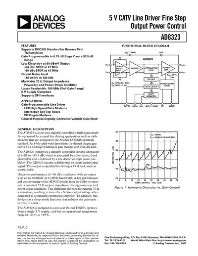
The AD8323 is a low‑cost, digitally controlled, variable‑gain line driver optimized for DOCSIS upstream applications such as cable modems and set‑top boxes. It provides a programmable gain range of about 53 dB in 0.75 dB steps, maintains a constant 75 Ω output impedance during power‑up and power‑down, and includes a sleep mode that reduces quiescent current to 4 mA.
The document includes full electrical specifications, pin descriptions, timing requirements, absolute maximum ratings, and layout guidelines. It also provides an evaluation board bill of materials, typical performance graphs, and application notes on SPI programming and power‑down operation.
| Input Resistance (Single‑Ended) | 800 Ω |
|---|---|
| Input Resistance (Differential) | 1600 Ω |
| Gain Range | 52.5 – 54.5 dB |
| Output Noise Spectral Density (Max Gain, 10 MHz) | 34 dBmV in 160 kHz |
| Power‑Supply Operating Range | 4.75 V – 5.25 V |
| Quiescent Current (Power‑Up Mode) | 133 mA (typical) |
| Sleep Mode Current | 4 mA (typical) |
| Operating Temperature Range | -40 °C to +85 °C |
Gain programming is performed via a serial peripheral interface (SPI) using the DATEN, SDATA, and CLK pins.
The device internally maintains a differential output impedance of 75 Ω regardless of forward or power‑down mode, eliminating the need for external termination resistors.
The PD pin (Logic 0) powers down the part, while the SLEEP pin (Logic 0) puts the device into low‑power sleep mode.
In power‑up mode the AD8323 draws about 133 mA of quiescent current.