
The LTC4556 provides all necessary power control, level translation and supervisory functions for a smart card or S.A.M. card interface. The part contains a low noise charge pump plus LDO for generating VCC power, as well as all necessary level shifting circuitry. The card voltage can be set to either 1.8V, 3V or 5V. The LTC4556 includes a card detection channel with automatic debounce circuitry. To reduce wiring costs, the LTC4556 interfaces to a microcontroller via a simple 4-wire serial interface. Multiple devices may be connected in daisy-chain fashion so that the number of wires to the card socket board is independent of the number of sockets. Status data is returned over the same interface. Extensive security features ensure proper deactivation sequencing in the event of a supply fault or a smart card electrical fault. The smart card pins can withstand greater than 10kV ESD in-situ with no additional components. The LTC4556 is available in a small, low profile (0.75mm), 4mm × 4mm QFN package.
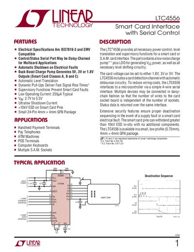
The LTC4556 provides power control, level translation and supervisory functions for smart‑card or SIM card interfaces. It includes a buck‑boost charge pump that can generate 5 V, 3 V or 1.8 V outputs and supports serial control for multiple card sockets.
The device is supplied in a 24‑lead 4 mm × 4 mm QFN package, operates from 2.7 V to 5.5 V input, and offers features such as automatic shutdown on faults, ESD protection over 10 kV, and a serial port capable of 10 MHz clock rates.
| Input voltage range | 2.7 V to 5.5 V |
|---|---|
| Operating current (typical) | 250 µA |
| Smart‑card output voltages | 5 V, 3 V, 1.8 V (or 0 V off) |
| ESD protection on smart‑card pins | >10 kV |
| Package | 24‑lead 4 mm × 4 mm Plastic QFN |
| Maximum serial clock rate | 10 MHz |
The serial port can operate up to 10 MHz.
It is supplied in a 24‑lead QFN package.
It can supply 5 V, 3 V, 1.8 V, or turn the supply off (0 V).
The pins are rated for greater than 10 kV ESD.