
This document describes the features and characteristics of the IRFR9N20D and IRFU9N20D SMPS MOSFET HEXFET® Power MOSFET products. They have a maximum drain-source voltage of 200V, maximum on-resistance of 0.38Ω, and maximum continuous drain current of 9.4A. Additionally, the document provides other parameters and absolute maximum ratings.
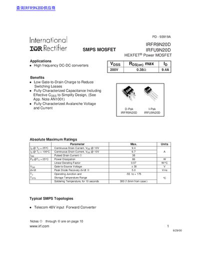
The IRFRON20D and IRFUSN20D are N‑channel HEXFET® power MOSFETs designed for high‑frequency DC‑DC converters and other switching applications. They feature low gate‑to‑drain charge to reduce switching losses and fully characterized capacitances to simplify design.
The document lists absolute maximum ratings, static and dynamic electrical characteristics, avalanche behavior, thermal resistance, and detailed package dimensions for D‑Pak (TO‑252AA) and I‑Pak (TO‑251AA) variants. It also includes typical test circuits, layout recommendations, and tape‑and‑reel handling information.
| Continuous Drain Current (Id) @ 25°C | 9.4 A |
|---|---|
| Continuous Drain Current (Id) @ 100°C | 6.7 A |
| Drain‑to‑Source Breakdown Voltage (Vds) | 200 V |
| Gate‑to‑Source Voltage (Vgs) Rating | +30 V |
| Total Gate Charge (Qg) | 18–27 nC |
| Input Capacitance (Ciss) | 560 pF |
| Output Capacitance (Coss) | 97 pF |
| Junction‑to‑Case Thermal Resistance (Rjc) | 1.75 °C/W |
| Single Pulse Avalanche Energy (Eas) | 100 mJ |
The device can conduct up to 9.4 A continuously at a drain‑to‑source voltage of 10 V.
The MOSFET is rated for a gate‑to‑source voltage of up to +30 V.
The typical turn‑on delay time is about 7.5 ns at Vpp = 100 V.