
The AD7887 is a 2-channel, 12-bit ADC with a voltage range of 2.7 V to 5.25 V. It operates at a micro-power level and has a sampling rate of 125 kSPS. It features flexible power/throughput rate management, a shutdown mode with a maximum current of 1 μA, and is suitable for battery-powered systems, instrumentation and control systems, and other applications.
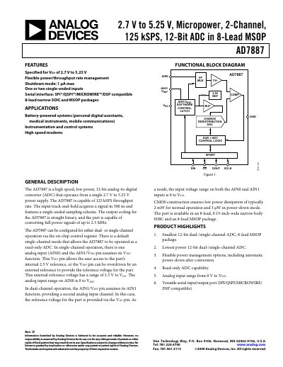
The AD7887 is a high‑speed, low‑power 12‑bit analog‑to‑digital converter that operates from a single 2.7 V to 5.25 V supply. It provides up to 125 kSPS conversion rate, with a flexible power‑down scheme and optional dual‑channel mode. The device includes an internal 2.5 V reference and supports both SPI‑compatible serial interfaces.
The part is available in 8‑lead narrow‑body SOIC and MSOP packages, operates over a temperature range of –40 °C to +125 °C, and meets stringent absolute‑maximum ratings for voltage, current, and ESD. Detailed specifications, timing diagrams, pin descriptions, and typical performance curves are provided for designers.
| Resolution | 12 bits |
|---|---|
| Throughput rate | 125 kSPS |
| Supply voltage (VDD) | 2.7 V to 5.25 V |
| Internal reference voltage | 2.5 V |
| Input voltage range (single‑channel) | 0 to VREF |
| Power consumption (shutdown mode) | 1 µA max |
| Package options | 8‑lead SOIC and 8‑lead MSOP |
The AD7887 can sample at up to 125 kSPS.
It operates from 2.7 V to 5.25 V supply voltage.
Yes, the AD7887 can be configured for either single‑channel or dual‑channel operation via the control register.
In shutdown mode the device draws as little as 1 µA (max) at 2.7 V to 3.6 V.