
The AD7339 is a composite IC that contains both DAC and ADC functions. The device includes an 8-bit parallel A-to-D converter. Two 8-bit parallel DACs are also included as are two serial control DACs. The AD7339, which operates with a single 5 V power supply, has a bandgap reference on board with a power-down mode.
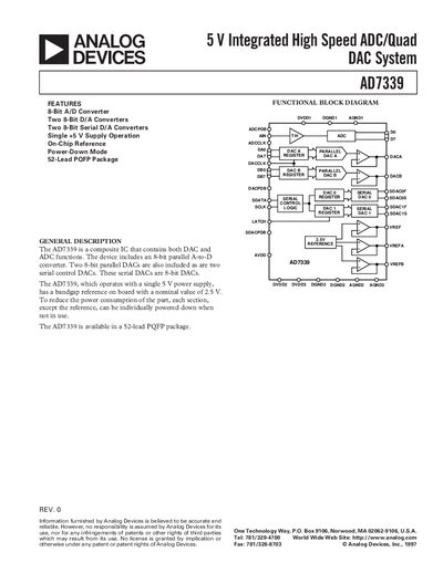
The AD7339 integrates an 8‑bit analog‑to‑digital converter, two 8‑bit parallel DACs, and two 8‑bit serial DACs in a 52‑lead PQFP package. It operates from a single +5 V supply and includes an on‑chip 2.5 V bandgap reference. Each functional block can be powered down independently to reduce consumption.
The document provides full electrical specifications, timing characteristics, absolute maximum ratings, pin configuration, grounding and layout recommendations, and ordering information for the AD7339.
| Resolution (ADC) | 8 Bits |
|---|---|
| Resolution (Parallel DACs) | 8 Bits |
| Resolution (Serial DACs) | 8 Bits |
| Conversion Rate (ADC) | 2.048 MSPS |
| Update Rate (Parallel DACs) | 2.304 MHz max |
| Update Rate (Serial DACs) | 256 kHz max |
| Input Voltage Range (ADC) | +1 V max |
| Reference Voltage | 2.5 V ±2 % (VREF) |
| Supply Voltage (AVDD/DVDD) | 4.5 V to 5.5 V |
| Operating Temperature Range | -40 °C to +85 °C |
The AD7339 operates from a single +5 V supply, with AVDD/DVDD allowed between 4.5 V and 5.5 V.
The ADC input can be driven up to +1 V maximum.
The device is specified for –40 °C to +85 °C operation.
The ADC conversion rate is 2.048 MSPS.