
The LTC660 is a monolithic CMOS switched-capacitor voltage converter. It performs supply voltage conversion from positive to negative from an input range of 1.5V to 5.5V, resulting in complementary output voltages of –1.5V to –5.5V. It also performs a doubling at an input voltage range of 2.5V to 5.5V, resulting in a doubled output voltage of 5V to 11V. Only two external capacitors are needed for the charge pump and charge reservoir functions. The converter has an internal oscillator that can be overdriven by an external clock or slowed down when connected to a capacitor. The oscillator runs at a 10kHz frequency when unloaded. A higher frequency outside the audio band can also be obtained if the BOOST pin is tied to V+. The LTC660 contains an internal oscillator, divide-by-two, voltage level shifter and four power MOSFETs. It is suitable for converting 5V to ±5V supplies, inexpensive negative supplies, data acquisition systems, and as a high current upgrade to LTC1044 or LTC7660.
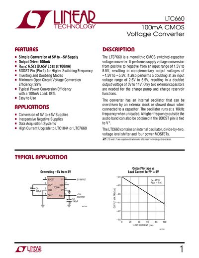
The LTC660 provides simple conversion of a positive supply to a negative output, or a doubled positive output, using an internal oscillator and four MOSFET switches. It operates from 1.5 V to 6 V input and delivers up to 100 mA with typical efficiency of 99 % at no load.
Typical applications include negative‑voltage inverters, voltage doublers, ultraprecision voltage dividers and battery splitters. The device is supplied in an 8‑lead SOIC package and includes pin functions for BOOST, CAP+, CAP‑, LV, OSC and Vout.
| Supply Voltage Range | 1.5 V to 6 V |
|---|---|
| Operating Temperature Range | 0 °C to 70 °C |
| Storage Temperature Range | -65 °C to 150 °C |
| Oscillator Frequency (BOOST open) | 10 kHz typical |
| Voltage Conversion Efficiency (no load) | 99 % (up to 99.96 %) |
With the BOOST pin open, the internal oscillator runs at about 10 kHz.
At no load the converter achieves roughly 99 % efficiency, up to 99.96 % in the best case.