
The LTC ®3423 and LTC3424 are high efficiency, fixed frequency, step-up DC/DC converters that can regulate output voltages as low as 1.5V from a single cell. An applied voltage of at least 2.7V to the VDD pin is required to power the internal control circuitry. The devices include a 0.16Ω N-channel MOSFET switch and a 0.21Ω P-channel synchronous rectifier. The LTC3423 is intended for applications requiring less than 0.75W of output power and the LTC3424 for 1.5W or less. Switching frequencies up to 3MHz are programmed with an external timing resistor and the oscillator can be synchronized to an external clock. Quiescent current is only 38µA in Burst Mode operation, maximizing battery life in portable applications. Burst Mode operation is user controlled and can be enabled by driving the MODE/SYNC pin high. If the MODE/SYNC pin has either a clock or is driven low then the operation is at constant fixed frequency. Other features include a 1µA shutdown, thermal shutdown and current limit. The LTC3423 and LTC3424 are available in the 10-lead MSOP package. For applications requiring an output voltage greater than 2.6V, the LTC3401 and LTC3402 are recommended without the need of a separate voltage for the VDD pin.
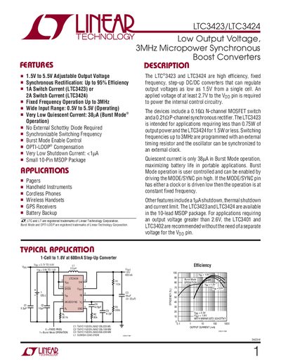
The LTC3423/LTC3424 series provides high‑efficiency step‑up conversion for portable applications. They operate from a wide input range of 0.5 V to 5.5 V and deliver adjustable output voltages from 1.5 V to 5.5 V. The devices feature synchronous rectification, fixed‑frequency operation up to 3 MHz, and very low quiescent current for battery‑powered designs.
Typical applications include handheld instruments, cordless phones, GPS receivers, and other low‑power wireless handsets. The parts include an internal N‑channel MOSFET switch and a P‑channel synchronous rectifier, and they support Burst Mode operation for ultra‑low standby power.
| Input Voltage Range | 0.5 V – 5.5 V |
|---|---|
| Output Voltage Adjust Range | 1.5 V – 5.5 V |
| Switch Current (LTC3423) | 1 A |
| Switch Current (LTC3424) | 2 A |
| Quiescent Current (Burst Mode) | 38 µA |
| Current Limit (LTC3423) | 1.6 A |
| Current Limit (LTC3424) | 2.8 A |
The devices operate from 0.5 V up to 5.5 V input.
Burst Mode is enabled by driving the MODE/SYNC pin high.
The shutdown current is less than 1 pA.
Typical quiescent current in Burst Mode is 38 µA.