
The MAX4214/MAX4215/MAX4217/MAX4219/MAX4222 are precision, closed-loop, gain of +2 (or -1) buffers featuring high slew rates, high output current drive, and low differential gain and phase error. They operate with a single 3.15V to 11V supply or with ±1.575V to ±5.5V dual supplies. The input common-mode voltage range extends 100mV beyond the negative power-supply rail, and the output swings Rail-to-Rail®. These devices require only 5.5mA of quiescent supply current while achieving a 230MHz -3dB bandwidth and a 600V/µs slew rate. In addition, the MAX4215/ MAX4219 have a disable feature that reduces the sup- ply current to 400µA per buffer. Input voltage noise is only 10nV/√Hz, and input current noise is only 1.3pA/√Hz. This buffer family is ideal for low-power/low- voltage applications requiring wide bandwidth, such as video, communications, and instrumentation systems. For space-sensitive applications, the MAX4214 comes in a miniature 5-pin SOT23 package.
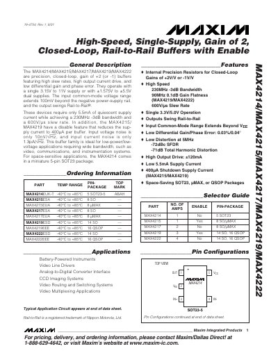
The MAX4214/5/7/9/4222 family are precision, closed‑loop buffers offering a gain of +2 (or –1), 230 MHz –3 dB bandwidth, and a 600 V/µs slew rate. They operate from a single 3.15 V to 11 V supply or dual ±1.575 V to ±5.5 V supplies, drawing only 5.5 mA quiescent current while delivering up to ±120 mA output drive.
These devices are suited for low‑power, wide‑bandwidth applications such as video, communications, and instrumentation. The MAX4215 and MAX4219 include an enable pin that reduces supply current to 400 µA when disabled, and the family supports rail‑to‑rail input and output swings with low differential gain and phase error.
| Gain | +2 (or -1) |
|---|---|
| Bandwidth | 230 MHz –3 dB |
| Slew Rate | 600 V/µs |
| Quiescent Supply Current | 5.5 mA per buffer |
| Shutdown Supply Current (disable) | 400 µA per buffer |
| Input Voltage Noise | 10 nV/√Hz |
| Input Current Noise | 1.3 pA/√Hz |
| Operating Supply Voltage (single) | 3.15 V to 11 V |
| Operating Temperature Range | -40 °C to +85 °C |
Each buffer draws about 5.5 mA of quiescent supply current.
The MAX4215 and MAX4219 have an enable pin; when disabled, the supply current drops to 400 µA per buffer.
The devices achieve a slew rate of 600 V/µs.
They operate from a single 3.15 V to 11 V supply or dual ±1.575 V to ±5.5 V supplies.