
The MAX9613/MAX9615 are low-power precision op amps with rail-to-rail inputs and rail-to-rail outputs. They feature precision MOS inputs powered from an internal charge pump to eliminate crossover distortion that is common to complementary input-pair type amplifier architectures. These devices are ideal for a large number of signal pro- cessing applications such as photodiode transimped- ance amplifiers and filtering/amplification of a wide variety of signals in industrial equipment.
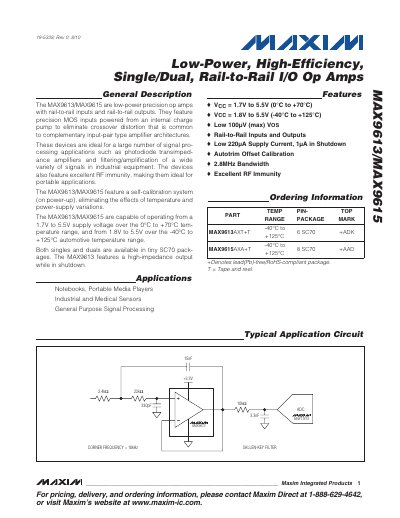
The MAX9613 and MAX9615 are low‑power precision operational amplifiers with rail‑to‑rail inputs and outputs. They feature an internal charge‑pump‑powered MOS input stage that eliminates crossover distortion, making them suitable for photodiode transimpedance amplifiers, active filters, and a wide range of industrial and portable signal‑processing applications.
The datasheet details supply voltage ranges, input offset voltage, bandwidth, quiescent current, and other key electrical parameters, and includes pin‑out diagrams, package information for SC70 packages, and typical operating characteristic curves.
| Supply Voltage Range | 1.7 V to 5.5 V (0 °C to +70 °C) |
|---|---|
| Supply Voltage Range (Automotive) | 1.8 V to 5.5 V (-40 °C to +125 °C) |
| Input Offset Voltage | ≤ 100 µV (max) |
| Gain‑Bandwidth | 2.8 MHz |
| Quiescent Current | 220 µA per amplifier (25 °C) |
| Output Voltage Low | 0.011 V at 10 kΩ load |
| Input Bias Current | 1.55 pA (typical) |
| Power‑Supply Rejection Ratio | 85 dB (typical at 25 °C) |
The devices operate from 1.7 V to 5.5 V for 0 °C to +70 °C, and from 1.8 V to 5.5 V for –40 °C to +125 °C automotive temperature ranges.
They use precision MOS inputs powered by an internal charge pump, which eliminates crossover distortion common in complementary input architectures.
The quiescent current is about 220 µA per amplifier at 25 °C.
The gain‑bandwidth product is 2.8 MHz.