
ORCA® Series 2 Field-Programmable Gate Arrays Data Sheet June 1999 is a high-performance, high-density, low-power field-programmable gate array. It has four-input look-up table (LUT) delay less than 1.0 ns of 0.35 µm CMOS technology (OR2CxxA), 0.3 µm CMOS technology (OR2TxxA) and 0.25 µm CMOS technology (OR2TxxB), and up to 43,200 usable, only logic gates; or 99,400 gates, including RAM.
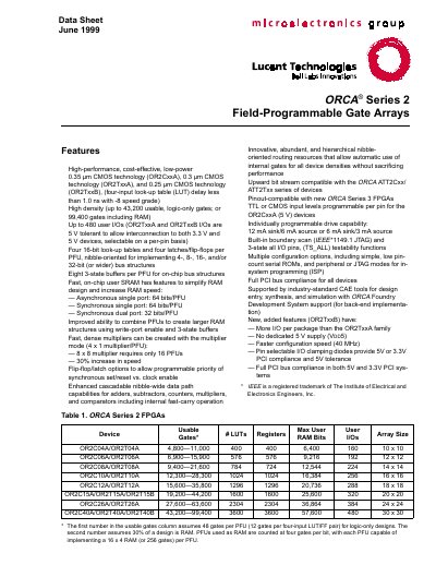
The ORCA Series 2 field‑programmable gate arrays are SRAM‑based devices built on 0.35 µm, 0.30 µm and 0.25 µm CMOS processes. They provide up to 43,200 usable logic‑only gates (99,400 including RAM) and feature four 16‑bit look‑up tables and four latches/flip‑flops per programmable function unit.
Each device contains up to 480 user I/Os, with selectable 3.3 V or 5 V tolerance, and supports multiple configuration modes including serial ROM, peripheral, and JTAG. The architecture includes programmable logic cells (PLCs) surrounded by programmable input/output cells (PICs), offering flexible routing and high‑speed arithmetic functions such as 4 × 1 multipliers and comparators.
| CMOS technology node | 0.35 µm (OR2CxxA), 0.30 µm (OR2TxxA), 0.25 µm (OR2TxxB) |
|---|---|
| Maximum usable gates | 43,200 logic‑only, 99,400 including RAM |
| User I/O pins | Up to 480 I/Os, 5 V tolerant per pin |
| Drive capability per I/O | 12 mA sink / 6 mA source (or 6 mA sink / 3 mA source) |
| PCI compliance | Full PCI bus compliance (5 V and 3.3 V systems) |
They are fabricated in 0.35 µm, 0.30 µm and 0.25 µm CMOS technologies.
Each device can provide up to 480 user I/Os, with each pin selectable for 3.3 V or 5 V operation.
Yes, the devices are fully PCI bus compliant for both 5 V and 3.3 V PCI systems.