
The CMOS 200 MSPS 14-Bit Quadrature Digital Upconverter AD9857 Rev. C is a high performance digital upconverter provided by Analog Devices, suitable for HFC data, telephony, and video modems, wireless base stations and other applications. The device features a 200 MHz internal clock rate, a 14-bit data path and excellent dynamic performance, providing 80 dB SFDR @ 65 MHz (±100 kHz) AOUT. The AD9857 also provides 4× to 20× programmable reference clock multipliers, reference clock multiplier PLL lock detect indicator, internal 32-bit quadrature DDS FSK capability, 8-bit output amplitude control, single-pin power-down function, four programmable, pin-selectable signal profiles, SIN(x)/x correction (inverse SINC function), simplified control interface, 10 MHz serial, 2-wire or 3-wire SPI®-compatible, 3.3 V single supply, single-ended or differential input reference clock and 80-lead LQFP surface-mount packaging.
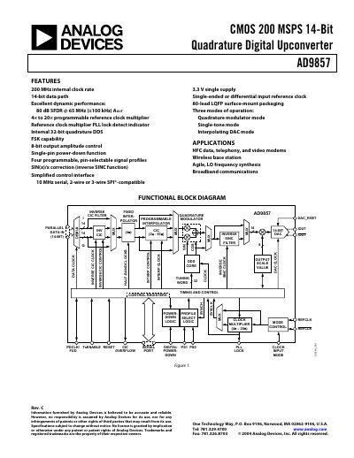
The AD9857 integrates a high‑speed direct digital synthesizer, a 14‑bit DAC, clock multiplier circuitry, and digital filters into a single chip, offering a universal I/Q modulator and agile upconverter for communications applications. It operates over an extended industrial temperature range of –40 °C to +85 °C and is supplied in an 80‑lead LQFP package.
The document includes a functional block diagram, detailed specifications, absolute maximum ratings, pin configuration tables, timing characteristics, power‑supply requirements, and an ordering guide, enabling designers to evaluate and implement the device in their systems.
| Internal clock rate | 200 MHz |
|---|---|
| Resolution | 14 Bits |
| Supply voltage | 3.3 V ± 5 % |
| Maximum junction temperature | 150 °C |
| Operating temperature range | –40 °C to +85 °C |
| Package type | 80‑lead LQFP (ST‑80) |
The device supports an internal clock rate of up to 200 MHz.
It is supplied in an 80‑lead quad flat‑pack (ST‑80) package.
The AD9857 operates from a 3.3 V single supply (±5 %).
It is rated for operation from –40 °C to +85 °C.