
The HIN202, HIN206, HIN207, HIN208, HIN211, HIN213 family of RS-232 transmitters/receivers interface circuits meet all ElA RS-232E and V.28 specifications, and are particularly suited for those applications where ±12V is not available. They require a single +5V power supply and feature onboard charge pump voltage converters which generate +10V and -10V supplies from the 5V supply. The family of devices offers a wide variety of RS-232 transmitter/receiver combinations to accommodate various applications (see Selection Table).
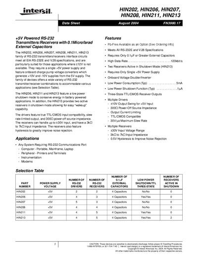
The HIN202, HIN206, HIN207, HIN208, HIN211 and HIN213 are +5 V powered RS‑232 transmitter/receiver ICs that generate +10 V and –10 V internal supplies. They meet all EIA RS‑232E and V.28 specifications and are suited for applications where a +12 V supply is unavailable.
The document provides detailed pin descriptions, pinout diagrams for various packages, absolute maximum ratings, electrical specifications, timing characteristics and mechanical dimensions for both standard and shrink‑size SOIC/SSOP packages.
| Supply voltage | +5 V (single supply) |
|---|---|
| Internal output voltage swing | +10 V / –10 V |
| No‑load supply current (typical) | 8 mA (HIN202) |
| Receiver input voltage range | -30 V to +30 V |
| Maximum junction temperature (plastic package) | 150 °C |
They operate from a single +5 V supply.
The typical no‑load current is about 8 mA.
The receivers accept input voltages from –30 V to +30 V.
The maximum junction temperature is 150 °C.