
This document describes the features and characteristics of STB25NM60N/-1, STF25NM60N, STP25NM60N, and STW25NM60N. These products have 100% avalanche tested, low input capacitance and gate charge, and low gate input resistance.
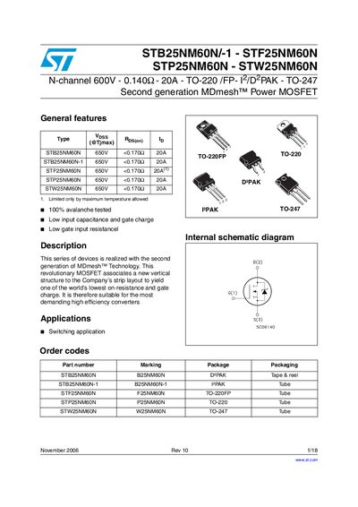
The STB25NM60N family comprises four N‑channel 600 V, 20 A Power MOSFETs built with ST's second‑generation MDmesh™ technology. The devices feature very low on‑resistance and gate charge, making them suitable for high‑efficiency switching converters.
The document provides absolute maximum ratings, detailed electrical characteristics, switching times, diode parameters, and mechanical data for the TO‑220, TO‑220FP, TO‑247 and DPAK packages. Revision history and legal notices are also included.
| Maximum drain‑source voltage (Vds) | 600 V |
|---|---|
| Avalanche current | 10 A |
| Input capacitance (Ciss) | 2540 pF |
The device is rated for a maximum drain‑source voltage of 600 V.
The avalanche current is rated at 10 A.