
The LTC1052 and LTC7652 are low noise zero-drift op amps manufactured using Linear Technology’s enhanced LTCMOS silicon gate process. Chopper-stabilization constantly corrects offset voltage errors. Both initial offset and changes in the offset due to time, temperature and common mode voltage are corrected. This, coupled with picoampere input currents, gives these amplifiers unmatched performance. Low frequency (1/f) noise is also improved by the chopping technique. Instead of increasing continuously at a 3dB/octave rate, the internal chopping causes noise to decrease at low frequencies. The chopper circuitry is entirely internal and completely transparent to the user. Only two external capacitors are required to alternately sample-and-hold the offset correction voltage and the amplified input signal. Control circuitry is brought out on the 14-pin and 16-pin versions to allow the sampling of the LTC1052 to be synchronized with an external frequency source.
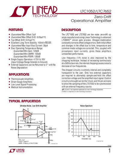
The LTC1052 and LTC7652 are low‑noise, zero‑drift operational amplifiers built with Linear Technology’s LTCMOS™ silicon‑gate process. They feature chopper‑stabilized offset correction, picoampere input bias currents, and single‑supply operation from 4.75 V to 16 V, delivering a guaranteed minimum gain of 120 dB.
The handbook details absolute maximum ratings, electrical characteristics, typical performance curves, theory of operation, recommended external capacitors, and package dimensions for both the 14‑lead PDIP (N) and 16‑lead plastic SO (SW) packages. It also includes application notes for thermocouple and strain‑gauge amplifiers and guidance on achieving picoampere/microvolt performance.
| Input Offset Voltage (Typical) | 5 µV |
|---|---|
| Input Bias Current (Typical) | 30 pA |
| Supply Current (No Load) | 2.0 mA |
| Gain Bandwidth Product | 1.2 MHz |
The guaranteed minimum gain is 120 dB.
It can operate from 4.75 V to 16 V on a single supply.
Typical input offset voltage is about 5 µV.