
The SPW34119D is a low power audio amplifier integrated circuit from SeCoSGmbH intended for telephone applications. It provides differential speaker outputs to max. output swing at low supply voltages (2V min.). Coupling capacitors to the speaker are not required. Open loop gain is 80dB, and the closed loop gain is set with two external resistors. A Chip Disable pin permits powering down and/or muting the input signal.
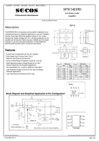
The SPW34119D is a low‑power audio amplifier IC intended primarily for telephone‑type speaker‑phone applications. It operates from 2 V to 16 V supply, provides differential speaker outputs without external coupling capacitors, and offers up to 250 mW output power into 32 Ω loads. The gain is adjustable from 0 dB to 46 dB using two external resistors, and a Chip Disable pin allows muting or power‑down.
The datasheet includes maximum ratings, recommended operating conditions, pin descriptions, electrical characteristics, design guidelines, and layout considerations. Graphs illustrate gain, power‑supply rejection, distortion, and device dissipation across load and supply conditions.
| Supply Voltage Range | 2 V to 16 V |
|---|---|
| Maximum Output Power | 250 mW into 32 Ω |
| Quiescent Supply Current | 2.7 mA typ. |
| Total Harmonic Distortion | 0.5 % typ. |
| Maximum Output Current | 250 mA |
| Load Impedance Range | 8 Ω to 32 Ω |
The device operates from a minimum of 2 V up to 16 V supply voltage.
It can deliver up to 250 mW of output power into a 32 Ω speaker load.
The typical quiescent supply current is 2.7 mA.