
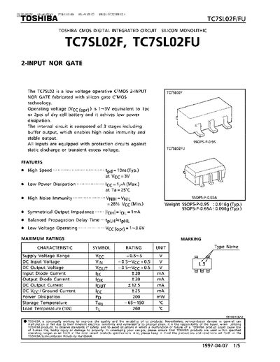
The TC7SLO2F/FU is a low‑voltage, low‑power CMOS 2‑input NOR gate with symmetrical output impedance and balanced propagation delay. It operates from 1 V to 3.6 V and includes input protection against static discharge.
The document lists maximum ratings, recommended operating conditions, DC and AC electrical characteristics, switching test results, package dimensions, and pin‑out diagrams for the SSOP5‑P‑0.95 and SSOP5‑P‑0.65 packages.
| Supply Voltage Range | 1 V ~ 3.6 V |
|---|---|
| Input Voltage Range | 0 V ~ VCC |
| Output Voltage Range | 0 V ~ VCC |
| Power Dissipation | 200 mW |
| Typical Package Weight (SSOP5‑P‑0.95) | 0.016 g |
| Typical Package Weight (SSOP5‑P‑0.65) | 0.006 g |
| Propagation Delay | Balanced tpLH = tpHL |
The device operates from 1 V to 3.6 V.
Typical power dissipation is 200 mW.
The propagation delay is balanced, with tpLH equal to tpHL.