
This document is TL494's technical documentation, which introduces the functional characteristics of TL494, including PWM power control circuit, uncommitted outputs, output control, internal circuitry, double pulses over total range, Easy synchronization, DIP-16, SOP-16, Pb-free plating, ordering information, pin configurations and block diagram.
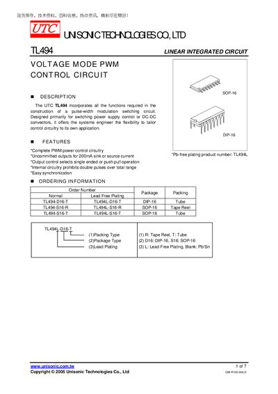
The TL494 linear integrated circuit provides all functions needed to build a pulse‑width‑modulation switching circuit, primarily for switching power‑supply control or DC‑DC converters. It features a voltage‑mode PWM control architecture with uncommitted outputs that can sink or source up to 200 mA, selectable single‑ended or push‑pull operation, and easy synchronization.
Key features include complete PWM power‑control circuitry, internal protection against double pulses, and a wide operating voltage range (7‑40 V). The device is offered in DIP‑16 and SOP‑16 packages (e.g., TL494‑D16‑T, TL494‑S16‑R) with lead‑free plating. Ordering information, pin configurations, and detailed electrical characteristics are provided in the datasheet.
| Supply Voltage (recommended) | 7 V – 40 V |
|---|---|
| Maximum Collector Output Voltage | 41 V |
| Collector Output Current (per transistor) | 200 mA |
| Oscillator Frequency | 1 kHz – 300 kHz |
| Unity‑Gain Bandwidth | 800 kHz |
| Package Types | DIP‑16 (TL494‑D16‑T) and SOP‑16 (TL494‑S16‑R/T) |
The maximum collector output voltage is 41 V.
The oscillator can operate from 1 kHz up to 300 kHz.
Each output can source or sink up to 200 mA.
The TL494 is offered in DIP‑16 (TL494‑D16‑T) and SOP‑16 (TL494‑S16‑R/T) packages.