
The ISL6161 is a HOT SWAP dual supply power distribution controller that can be used in PCI-Express applications. Two external N-Channel MOSFETs are driven to distribute and control power while providing load fault isolation. At turn-on, the gate of each external N-Channel MOSFET is charged with a 10µA current source. Capacitors on each gate (see the Typical Application Diagram), create a programmable ramp (soft turn-on) to control inrush currents. A built-in charge pump supplies the gate drive for the 12V supply N-Channel MOSFET switch. Over current protection is facilitated by two external current sense resistors and FETs. When the current through either resistor exceeds the user programmed value the controller enters the current regulation mode. The time-out capacitor, CTIM, starts charging as the controller enters the time out period. Once CTIM charges to a 2V threshold, both the N-Channel MOSFETs are latched off. In the event of a hard and fast fault of at least three times the programmed current limit level, t
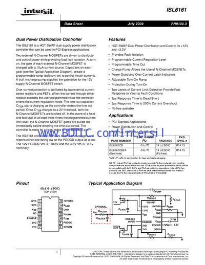
The ISL6161 provides hot‑swap dual power distribution for +12 V and +3.3 V rails. It drives external N‑Channel MOSFETs, offers programmable current‑limit thresholds, time‑out control, and includes a charge pump for gate drive. The device includes power‑good and over‑current latch indicators and supports soft turn‑on ramp control.
Typical applications include PCI‑Express add‑in cards and other power‑distribution designs. The datasheet details pin functions, absolute maximum ratings, electrical specifications, package dimensions, and performance curves to aid designers in implementing the controller.
| Supply Voltage Range (Vpp) | +10.5 V to +13.2 V |
|---|---|
| Operating Temperature Range | -65 °C to 150 °C |
| Maximum Junction Temperature | 150 °C |
| Current Limit Threshold Voltage (12 V, 10 kΩ sense resistor) | 92 mV (min) – 108 mV (max) |
The ENABLE pin turns the device on when driven low and resets it with a rising edge; it also provides a pull‑up for open‑drain operation.
The ISL6161 is reset by a rising edge on the ENABLE pin.
The charge pump supplies the gate‑drive voltage for the external 12 V N‑Channel MOSFET switch.