
The document describes the features of ADA4627-1/ADA4637-1 JFET operational amplifiers, including low offset voltage, low offset drift, low input bias current, high slew rate, high gain, etc.
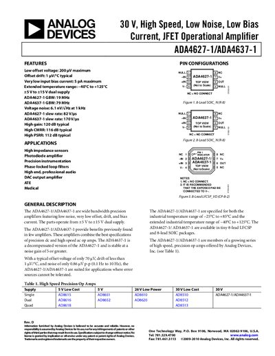
The ADA4627-1 and ADA4637-1 are high‑speed precision operational amplifiers featuring low offset voltage, very low input bias current, and wide bandwidth. They operate from ±5 V to ±15 V dual supplies and are available in 8‑lead SOIC and LFCSP packages.
The document provides detailed electrical characteristics, absolute maximum ratings, typical performance graphs, and ordering information for both devices, covering temperature ranges from –40 °C to +125 °C and various application notes such as high‑impedance sensors and audio DAC output stages.
| Low offset voltage | 200 µV maximum |
|---|---|
| Gain Bandwidth Product (GBW) | 19 MHz (ADA4627‑1) / 79 MHz (ADA4637‑1) |
| Slew Rate | 82 V/µs (ADA4627‑1) / 170 V/µs (ADA4637‑1) |
| Supply voltage range | ±5 V to ±15 V dual supply |
| Operating temperature range | −40 °C to +125 °C |
The ADA4627-1 has a typical offset voltage of 200 µV maximum.
Both devices are specified to operate from –40 °C to +125 °C.
They operate from ±5 V to ±15 V dual supply.
The ADA4627-1 has a GBW of 19 MHz, while the ADA4637-1 has a GBW of 79 MHz.