
The CDCU877 is a high-performance, low-jitter, low-skew, zero-delay buffer that distributes a differential clock input pair (CK, CK) to ten differential pairs of clock outputs (Yn, Yn) and one differential pair of feedback clock output (FBOUT, FBOUT). The clock outputs are controlled by the input clocks (CK, CK), the feedback clocks (FBIN, FBIN), the LVCMOS control pins (OE, OS) and the analog power input (AVDD). When OE is low, the clock outputs, except FBOUT/FBOUT, are disabled while the internal PLL continues to maintain its locked-in frequency. OS (output select) is a program pin that must be tied to GND or VDD. When OS is high, OE functions as previously described. When OS and OE are both low, OE has no affect on Y7/Y7, they are free running.
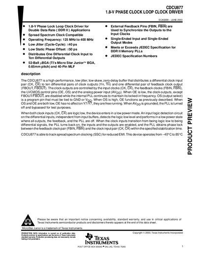
The CDCU877 is a high‑performance, low‑jitter, low‑skew, zero‑delay buffer that distributes a differential clock input pair (CK, CK) to ten differential clock outputs (Yn, Yn) and a feedback output pair (FBOUT, FBOUT). Output enable (OE) and output select (OS) pins allow control of the driver, while the internal PLL maintains lock to the reference clock.
The device operates from –40 °C to 85 °C, supports spread‑spectrum clocking, and includes specifications for supply voltage, input/output voltage ranges, timing parameters, and mechanical dimensions. Detailed electrical characteristics, timing requirements, and switching characteristics are provided for design verification.
| Operating Frequency | 125 MHz to 400 MHz |
|---|---|
| Supply Voltage (Vpp) | 1.7 V to 1.9 V |
The CDCU877 operates from 125 MHz up to 400 MHz.
The device requires a supply voltage (Vpp) between 1.7 V and 1.9 V.