
Key facts
- Manuals
- 1
- Languages
- EN
- Last added
- 2012-01-04
Featured CDCU877 manuals
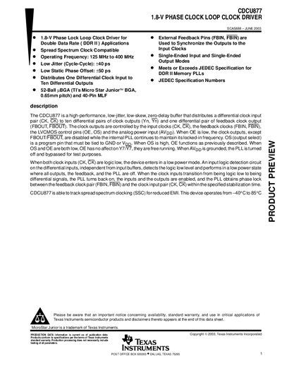
Texas Instruments CDCU877 1.8‑V Phase Clock Loop Clock Driver Datasheet
The CDCU877 is a high‑performance, low‑jitter, low‑skew, zero‑delay buffer that distributes a differential clock input pair (CK, CK) to ten differential clock outputs (Yn, Yn) and a feedback output pair (FBOUT, FBOUT). Output enable (OE) and output select (OS) pins allow control of the driver, while the internal PLL maintains lock to the reference clock.
The device operates from –40 °C to 85 °C, supports spread‑spectrum clocking, and includes specifications for supply voltage, input/output voltage ranges, timing parameters, and mechanical dimensions. Detailed electrical characteristics, timing requirements, and switching characteristics are provided for design verification.
Covers: Product Overview · Terminal Functions · Electrical Characteristics · Timing Requirements · Switching Characteristics · Mechanical Data
Latest CDCU877 manuals
Texas Instruments CDCU877 1.8‑V Phase Clock Loop Clock Driver Datasheet
Datasheet 15 pages · 257 KB · ENThe CDCU877 is a 1.8‑V phase‑locked loop clock driver from Texas Instruments, delivering low‑jitter distribution of differential clock signals to up to ten…
Which document do I need?
Datasheet
Ratings, dimensions and ordering codes, for selection and design work.
Questions answered in CDCU877 manuals
What is the operating frequency range of the CDCU877?
The CDCU877 operates from 125 MHz up to 400 MHz.
From: Texas Instruments CDCU877 1.8‑V Phase Clock Loop Clock Driver Datasheet
What supply voltage does the CDCU877 require?
The device requires a supply voltage (Vpp) between 1.7 V and 1.9 V.
From: Texas Instruments CDCU877 1.8‑V Phase Clock Loop Clock Driver Datasheet