
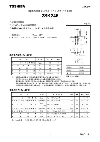
The 2SK246 is a silicon N‑channel junction field‑effect transistor (JFET) intended for constant‑current circuits, impedance‑conversion stages, and various DC‑AC high‑impedance amplification applications. The device offers high breakdown voltage and low leakage current, making it suitable for precision analog designs.
The datasheet lists absolute maximum ratings such as a -50 V gate‑drain voltage, 10 mA drain current, and 300 mW power dissipation, as well as recommended operating conditions and reliability guidelines. Users are advised to consult Toshiba’s semiconductor reliability handbook for derating and safety design considerations. This manual is written in Japanese.
| Gate‑Drain Breakdown Voltage (Vgd) | -50 V |
|---|---|
| Drain Current (Idss) | 5.6 mA |
| Power Dissipation (Pd) | 300 mW |
| Maximum Junction Temperature | 125 °C |
| Storage Temperature Range | -55 °C to 125 °C |
| Maximum Drain Current (Id) | 10 mA |
The maximum gate‑drain voltage is -50 V.
The device can handle up to 10 mA of drain current.
The recommended storage temperature range is -55 °C to 125 °C.