
ADP2503/ADP2504 is a high efficiency, low static current boost/buck DC-DC converter that can operate when the input voltage is greater than, less than or equal to the regulated output voltage. The built-in switch and synchronous rectifier minimize external component count. When load current is high, ADP2503/ADP2504 employs a current mode fixed frequency PWM (pulse width modulation) control scheme for excellent stability and transient response. To extend battery life in portable applications, ADP2503/ADP2504 features an optional power saving mode that reduces switching frequency under light load conditions. For wireless and other low noise applications where variable frequency power saving mode may cause interference, a logic control input sync can force fixed frequency PWM operation under all load conditions. ADP2503/ADP2504 input voltage range of 2.3 V to 5.5 V allows use with single lithium or lithium polymer battery
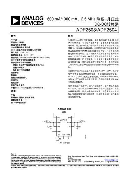
The ADP2503/ADP2504 are high‑efficiency, low‑static‑current buck‑boost DC‑DC converters that operate over a wide input range (2.3 V‑5.5 V) and provide fixed output voltages from 2.8 V to 5 V. They support three operating modes – Power‑Save Mode (PSM), forced PWM, and synchronization mode – to optimize efficiency across load conditions. Typical applications include mobile phones, digital cameras, portable audio players, and USB‑powered devices.
The datasheet details pin configuration for the 10‑pin LFCSP/QFN package, provides absolute maximum ratings, thermal resistance, ESD warnings, and recommended external components such as input capacitors. It also includes PCB layout guidelines, performance graphs, and an ordering guide for various voltage/current variants. This manual is written in Chinese.
| Output current (ADP2503) | 600 mA |
|---|---|
| Static current | 38 µA – 50 µA |
| Switching frequency | 2.5 MHz |
ADP2503 can deliver up to 600 mA, while ADP2504 can deliver up to 1000 mA.