
IBM's manual details specifications, pin assignments, operation modes, and initialization procedures for the 128Mb Synchronous DRAM devices.
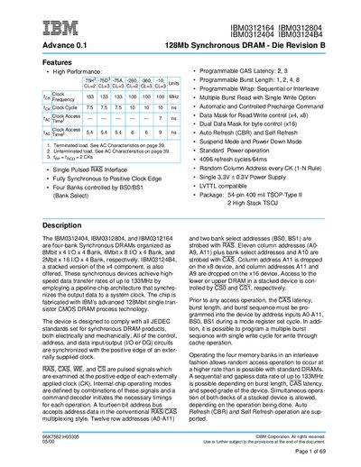
The document describes the IBM 128Mb Synchronous DRAM family (part numbers IBM0312164, IBM0312804, IBM0312404, IBM03124B4). It covers features such as high‑performance single‑pulsed RAS interface, programmable CAS latency and burst length, and power‑down modes. Pin assignments, functional descriptions, and block diagrams for both planar and stacked packages are provided.
Operational details include the power‑on and initialization sequence, mode register programming, burst‑mode operation, and ordering information. Package dimensions and revision history are also listed, along with legal notices and IBM contact information.
| Clock Frequency | 133 MHz |
|---|---|
| CAS Latency | 2 or 3 cycles |
| Burst Length | 1, 2, 4, or 8 |
| Power Supply Voltage | 3.3 V ±0.3 V |
| Package Type | 54‑pin 400 mil TSOP‑Type II |
| Refresh Cycles | 4096 cycles per 64 ms |
The device operates from a single 3.3 V ±0.3 V power supply.
The DRAM performs 4096 refresh cycles every 64 ms.
CAS latency can be programmed to either 2 or 3 clock cycles.
Burst length can be set to 1, 2, 4, or 8.