
Hitachi S-3000 series scanning electron microscope leaflet covering the S-3600N resolution, sample capacity, 5-axis stage and imaging features.
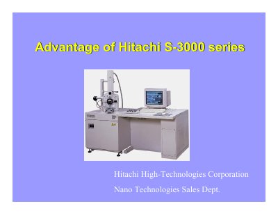
This leaflet from Hitachi High-Technologies Corporation, Nano Technologies Sales Dept., presents the advantages of the Hitachi S-3000 series of scanning electron microscopes, using model S-3600N as the example. It lists a resolution of 3.0 nm in HV mode, 30 nm at 3 kV with Dual bias mode, and 4.5 nm in VP mode, together with a maximum sample size of 10 inch fai (254 mm), sample thickness up to 70 mm, sample weight up to 2.0 kg and a 5-axis automatic stage with X/Y travel of 150 mm/110 mm.
Feature pages describe the TV Scan mode and Full Screen function, the Capture button and Capture box for storing live images as digital data, a 4-segment semiconductor type BSE detector, high-contrast imaging at low accelerating voltage with the Dual Bias function, a maintenance assist function with a 3D CG maintenance guide, and the ESED Environment Secondary Electron Detector. Several pages compare these points with the JEOL JSM-6460LV and JSM-6xxx series, and the closing pages compare BSE and ESED images of encapsulated fat particles, a rubber roller surface and calcium carbonate.
| Resolution (HV mode) | 3.0 nm |
|---|---|
| Resolution (VP mode) | 4.5 nm |
| Low accelerating voltage resolution guarantee | 30 nm at 3 kV (with Dual bias mode) |
| Maximum sample size | 10 inch fai (254 mm fai) |
| Maximum sample thickness | 70 mm |
| Maximum sample weight | 2.0 kg |
| Stage | 5 axis auto large stage, X/Y: 150 mm/110 mm |
| Full screen display | 1,024 x 768 pixels |
| TV scan rate | 0.033 sec./frame |
3.0 nm in HV mode, 30 nm at 3 kV with Dual bias mode, and 4.5 nm in VP mode.
Samples up to 10 inch fai (254 mm fai) can be accommodated, with a maximum sample weight of 2.0 kg.
The maximum sample thickness capability is 70 mm.
ESED stands for Environment Secondary Electron Detector.