
The Cadence Xtensa LX6 Customizable DPU datasheet describes its configurable architecture, I/O options, memory, power and debug features.
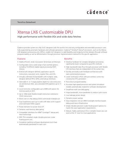
The Xtensa LX6 Customizable DPU is a 32‑bit configurable processor core that can be tailored with pre‑verified options such as DSP blocks, floating‑point units, and wide I/O interfaces. Designers can add application‑specific instructions, execution units and registers using the Tensilica Instruction Extension (TIE) methodology, and the tool chain automatically generates matching RTL and software support.
The core supports multiple pipeline depths (5‑ or 7‑stage), up to 128‑bit wide FLIX instructions, configurable local memories up to 8 MB with parity/ECC, and up to 32 interrupt sources. Power domains, semantic and data gating, and fine‑grained clock gating enable low‑leakage operation. Debug is provided via multi‑core on‑chip debug (OCD) with CoreSight‑compatible interfaces and optional performance counters.
| Base architecture | 32‑bit |
|---|---|
| Local memory size | Up to 8 MB (optional parity/ECC) |
| Instruction width | Up to 128 bits (FLIX) |
| Interrupts | Up to 32 interrupts with seven priority levels |
| Cache configuration | Up to 4‑way set associative, up to 128 KB |
| Pipeline depth | Selectable 5‑ or 7‑stage (DSP pipelines up to 11 stages) |
| Power domains | Supported for power shut‑off |
The core offers a selectable 5‑ or 7‑stage pipeline, and optional DSP pipelines can be extended up to 11 stages.
Local memories can be configured up to 8 MB, with optional parity or ECC protection.
The DPU supports up to 32 interrupts, each with up to seven priority levels plus a non‑maskable interrupt.