
The ADP5020 is a highly integrated power management unit with two buck converters, an LDO and I²C control for imaging modules.
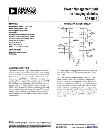
The ADP5020 provides a compact power solution for digital imaging modules, integrating two step‑down DC‑DC converters, a low‑dropout regulator, and a power‑sequence controller. It operates from 2.4 V to 5.5 V and can be programmed via an I²C interface or an enable pin.
Key features include a 3 MHz switching frequency, low standby current (1 µA), synchronous buck converters (600 mA and 250 mA), and a 150 mA LDO. The device is supplied in a 20‑lead LFCSP package (4 mm × 4 mm) and supports a wide temperature range from –40 °C to +125 °C.
| Input voltage range | 2.4 V to 5.5 V |
|---|---|
| Low standby current | 1 µA |
| Switching frequency | 3 MHz |
| Buck 1 regulator max current | 600 mA |
| Buck 2 regulator max current | 250 mA |
| LDO max current | 150 mA |
| Operating temperature range (junction) | ‑40 °C to +125 °C |
| Package | 20‑lead LFCSP (4 mm × 4 mm) |
The device operates from 2.4 V to 5.5 V.
It draws a typical standby current of 1 µA.
Both buck converters run at a fixed 3 MHz switching frequency.
It includes two step‑down buck converters and one low‑dropout regulator.