
This guide introduces the basic features of the LPC2468 Developer's Kit and provides detailed instructions on how to use the kit to develop your own applications.
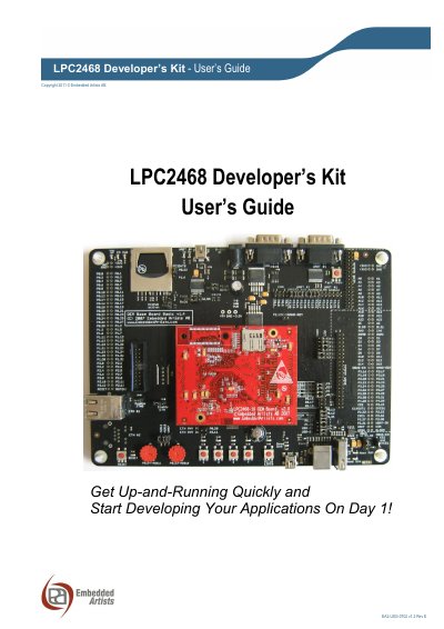
The LPC2468 Developer's Kit is based on NXP's ARM7TDMI-S LPC2468 microcontroller and consists of the LPC2468 OEM Board and the OEM Base Board Basic. The guide covers both 16- and 32-bit data bus versions of the OEM Board and describes the base board hardware design.
It documents board features including external FLASH and SDRAM, Ethernet, USB-OTG, uSD/transflash, expansion connectors, jumpers and connectors. It also covers the QVGA display add-on board, initial setup and powering, LAN/Ethernet setup and the FTDI USB driver.
| Microcontroller | NXP ARM7TDMI-S LPC2468 |
|---|---|
| Program FLASH | 512 KByte |
| SRAM | 96 KByte |
| External FLASH | 128 MB NAND FLASH and 4 MB NOR FLASH |
| External data memory | 32 MB SDRAM |
| Main crystal | 12.0000 MHz |
| RTC crystal | 32.768kHz |
| Ethernet interface | 100/10M Ethernet PHY/interface |
| I2C E2PROM | 256 Kbit |
| OEM Board dimensions | 80 x 65 mm (16-bit); 75 x 40 mm (32-bit) |
It consists of the LPC2468 OEM Board and the OEM Base Board Basic.
The board uses NXP's ARM7TDMI-S LPC2468 microcontroller in a BGA package.
It can be powered via USB or an external 9-15V DC supply.
First touch the metal surface of a USB connector for a few seconds with both hands before touching other parts.