
The L6560/A is a monolithic integrated circuit designed as a controller and driver of a discrete power MOS transistor for the implementation of active power factor correction, for sinusoidal line current consumption. The chip is realized in mixed BCD technology, and integrates: an undervoltage lockout with micropower start-up and hysteresis, an internal temperature compensated precise band gap reference, a stable error amplifier, one quadrant multiplier, current sense comparator, an output overvoltage protection circuit, and a totem-pole output stage able to drive a POWER MOS or IGBT devices with source and sink current of 400mA. The chip works in transition mode and is particularly intended for lamp ballast applications and for low power SMPS.
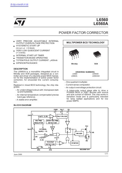
The L6560 and L6560A are monolithic integrated circuits available in Minidip and SO8 packages. Designed as a controller and driver for a discrete power MOS transistor, they are intended for the implementation of active power factor correction to achieve sinusoidal line current consumption. The chips are particularly suited for lamp ballast applications and low power SMPS.
| Package Types | Minidip and SO8 |
|---|---|
| Totem Pole Output Current | +400mA |
| Quiescent Current | <3.5mA |
| Operating Junction Temperature | -25 to 150 °C |
| Error Amplifier Voltage Gain | 60 to 80 dB |
It is designed as a controller and driver for a discrete power MOS transistor for active power factor correction.
The maximum operating junction temperature is 150 °C.
The typical quiescent current is less than 3.5mA.