
The document describes an advanced high-speed CMOS octal D-type flip-flop with 3-state outputs. It is fabricated with sub-micron silicon gate and double-layer metal wiring C2MOS technology. This flip-flop consists of a clock input and an output enable input to control its operation. On the positive transition of the clock, the Q outputs will reflect the logic states that were set up at the D inputs. When the output enable input is low, the 8 outputs will be in a normal logic state (high or low logic level), and when the output enable input is high, the outputs will be in a high impedance state. The output control does not affect the internal operation of the flip-flop, allowing the retention of old data or the input of new data even when the outputs are off. Power down protection is provided on all inputs and outputs, and inputs can accept voltages from 0 to 7V regardless of the supply voltage. This device can be used to interface 5V to 3V as all inputs are equipped with TTL threshold.
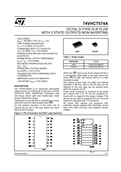
The 74VHCT574A is an advanced high-speed CMOS octal D-type flip-flop with 3-state non-inverting outputs, fabricated with sub-micron silicon gate and double-layer metal wiring CMOS technology. It features high-speed operation with a typical frequency of 180 MHz at 5V and low power dissipation of 4 mW maximum at 25°C.
| Low Power Dissipation | 4 mW (Max) at Ta=25°C |
|---|---|
| Operating Voltage Range | 4.5V to 5.5V |
| Supply Voltage | 4.5 to 5.5 V |
| Operating Temperature | -55 to 125 °C |
| Package Types | SOP, TSSOP |
Yes, it is compatible with TTL outputs with a minimum input voltage of 2V.
Yes, power down protection is provided on all inputs and outputs.