
The M74HC367 is a high-speed CMOS HEX BUS BUFFER with 3-state outputs fabricated with silicon gate C2MOS technology. This device contains six buffers, four buffers are controlled by an enable input (G1) and the other two buffers are controlled by the other enable input (G2); the outputs of each buffer group are enabled when G1 and/or G2 inputs are held low, and when held high, these outputs are disabled in a high-impedance state. All inputs are equipped with protection circuits against static discharge and transient excess voltage.
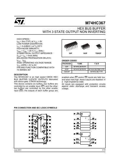
The M74HC367 is a high-speed CMOS hex bus buffer fabricated with silicon gate C2MOS technology. It contains six buffers, where four are controlled by an enable input (G1) and the other two by a separate enable input (G2). When the enable inputs are held low, the outputs are active; when held high, the outputs enter a high-impedance state. All inputs include protection circuits against static discharge and transient excess voltage.
| Supply Voltage Range | 2V to 6V |
|---|---|
| Propagation Delay (Typical) | 9ns |
| Power Dissipation (Max) | 4mW |
| Operating Temperature | -55 to 125 °C |
| Output Current (Max) | +35 mA |
| Input Capacitance | 5 pF |
Yes, it is pin and function compatible with 74 series 367.
The device contains six buffers.
The typical propagation delay is 9ns at 6V.