
The M74HC4049 is a high-speed CMOS Hex Buffer (Inverting) fabricated with silicon gate C2MOS technology. The internal circuit is composed of 2 stage inverters, which enables high noise immunity and a stable output. Input protection circuits are different from those of the high speed CMOS IC's. The Vcc side diodes are designed to allow logic-level conversion from high-level voltages (up to 13V) to low level voltages.
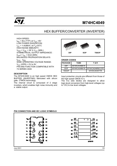
This document is a datasheet for the M74HC4049, a high-speed CMOS hex buffer (inverting) fabricated with silicon gate CMOS technology. The device features high noise immunity, symmetrical output impedance, and balanced propagation delays, operating with a wide voltage range from 2V to 6V.
| Supply Voltage Range | 2V to 6V |
|---|---|
| High Speed Propagation Delay | 8ns (Typ.) at 6V |
| Maximum Power Dissipation | 1mW |
| Operating Temperature Range | -55 to 125 °C |
| Input Capacitance | 5 pF |
The absolute maximum supply voltage rating is +7V.
Yes, it is pin and function compatible with the 74 series 4049.
The device is available in DIP, SOP, TSSOP, and T&R packages.