
VND5050J-E VND5050K-E double channel high side driver for automotive applications. The features of the driver include: main inrush current active management by power limitation, very low standby current, 3.0 V CMOS compatible input, optimized electromagnetic emission, very low electromagnetic susceptibility, compliance with the 2002/95/EC European directive, diagnostic functions, open drain status output, on-state open load detection, off-state open load detection, thermal shutdown indication, undervoltage shutdown, overvoltage clamp, output stuck to VCC detection, load current limitation, self limiting of fast thermal transients, protection against loss of ground and loss of VCC, thermal shutdown, reverse battery protection (see Figure 28) and electrostatic discharge protection. Applications include all types of resistive, inductive and capacitive loads
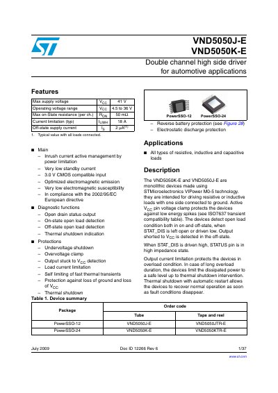
The VND5050J-E and VND5050K-E are monolithic double channel high side drivers designed for automotive applications using STMicroelectronics VIPower MO-5 technology. These devices are intended for driving resistive or inductive loads with one side connected to ground and feature active Voc pin voltage clamp protection against low energy spikes.
| Max supply voltage Veco | 4 V |
|---|---|
| Operating voltage range Voc | 4.5 to 36 V |
| Max on-State resistance (per ch.) | 50 mQ |
| Current limitation (typ) | 18A |
| Junction operating temperature | -40 to 150 °C |
The operating supply voltage range is from 4.5 V to 36 V.
The maximum on-state resistance is 50 mQ per channel.
Yes, the device includes reverse battery protection, though an external diode or resistor is required in the ground line.