
This document describes the Latch-Up phenomenon in CMOS logic, including the causes, consequences, and how to prevent Latch-Up
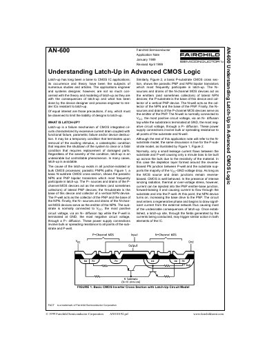
Latch-up is a failure mechanism in CMOS integrated circuits characterized by excessive current drain and potential device destruction. It arises from parasitic PNPN paths inherent in junction-isolated or bulk CMOS processes, involving lateral PNP and vertical NPN bipolar transistors.
The document details the conditions necessary for latch-up to occur, including biasing both parasitic bipolars into the active state and sufficient loop gain. It outlines precautions such as using current-limited power supplies, series resistors, and proper layout techniques to reduce susceptibility and prevent damage.
Latch-up is a failure mechanism of CMOS integrated circuits characterized by excessive current drain coupled with functional failure, parametric failure and/or device destruction.
Both parasitic bipolars must be biased into the active state; the product of their current gains must be greater than or equal to one; and the terminal network must supply a current greater than the holding current.
Prevention involves preventing biasing of bipolars into the active region and limiting the current supplied by the network, using measures like diode clamping and series limiting resistors.