
The MC33253 is a full bridge driver including integrated charge pump, two independent high and low side driver channels. The high and low side drivers include a cross conduction suppression circuit, which, if enabled, prevents the external power FETs from being on at the same time. The drive outputs are capable to source and sink 1 A pulse peak current. The low side channel is referenced to ground, the high side channel is floating above ground. A linear regulator provides a maximum of 15.5V to supply the low side gate driver stages. The high side driver stages are supplied with a 10V charge pump voltage. Such built-in feature, associated to external capacitor provides a full floating high side drive. An under- and over-voltage protection prevents erroneous operation.
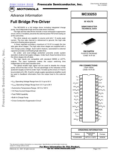
The MC33253 is a full bridge driver that includes an integrated charge pump and two independent high and low side driver channels. It features a cross conduction suppression circuit to prevent external power FETs from being on simultaneously, along with under- and over-voltage protection.
Key specifications include the ability to source and sink 1 A pulse peak current, operation within a Vcc range of 5.5 V up to 55 V, and an automotive temperature range of -40°C to +125°C.
| Supply Voltage Range (Vcc) | 5.5 V to 55 V |
|---|---|
| Output Driver Current | 1 A Pulse Peak |
| Operating Temperature Range | -40°C to +125°C |
| Quiescent Supply Current (Shutdown) | Under 10uA |
It prevents the external power FETs from being on at the same time.
It provides a maximum of 15.5V to supply the low side gate driver stages.