
This paper introduces a systematic approach to design high-performance bootstrap gate drive circuits for high-frequency, high-power, and high-efficiency switching applications.
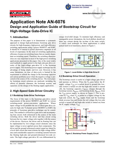
This document provides a systematic approach to designing bootstrap gate drive circuits for high-frequency, high-power, and high-efficiency switching applications using power MOSFETs and IGBTs. It focuses on the bootstrap power supply technique, which is widely used for its simplicity and low cost in high-side gate drive circuitry.
The guide analyzes the operation of the bootstrap circuit, including the charging of the bootstrap capacitor through a resistor and diode. It details the limitations of this technique, such as duty-cycle restrictions due to capacitor refresh requirements and issues arising from negative voltage transients at the source terminal. The document also covers potential problems like latch-up caused by parasitic elements and provides theoretical extremes to understand the relationships between excessive undershoot and latch-up mechanisms.
The document demonstrates a systematic approach to design high-performance bootstrap gate drive circuits for high-frequency, high-power, and high-efficiency switching applications using a power MOSFET and IGBT.
The bootstrap power supply technique has the advantage of being simple and low cost.
The gate drive IC suffers damage or temporarily latches in its current state.