
The document describes the features and characteristics of the 74LCX125 low voltage quad buffer, including 5V tolerant inputs and outputs, 2.3V-3.6V VCC specifications, maximum propagation delay of 6.0ns (VCC = 3.3V), maximum input current of 10µA, support for live insertion/withdrawal, ±24mA output drive (VCC = 3.0V), latch-up performance exceeding JEDEC 78 conditions, and ESD performance.
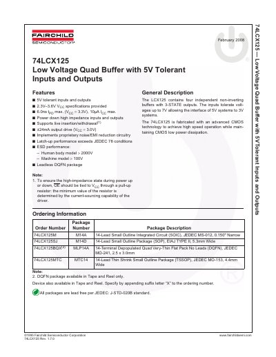
The 74LCX125 is a low voltage quad buffer featuring four independent non-inverting buffers with 3-STATE outputs. It is fabricated with advanced CMOS technology to achieve high-speed operation while maintaining low power dissipation. The device includes proprietary noise and EMI reduction circuitry and supports live insertion and withdrawal.
| Supply Voltage | 2.3V to 3.6V |
|---|---|
| Propagation Delay | 6.0ns max |
| Output Drive | +24mA |
| Input Tolerance | 5V |
| Operating Temperature | -40°C to +85°C |
The device operates with a supply voltage between 2.0V and 3.6V.
The maximum propagation delay is 6.0ns when the supply voltage is 3.3V.