
This document describes the application of zero voltage crossing optically isolated triac drivers in interface applications. These drivers are low-cost, simple and effective solutions for interfacing between low current DC control circuits such as logic gates and microprocessors and AC power loads (120, 240 or 380 volt, single or 3-phase). They provide sufficient gate trigger current for high current, high voltage thyristors, while providing a guaranteed 7.5 kV dielectric withstand voltage between the line and the control circuitry. An integrated, zero-crossing switch on the detector chip eliminates current surges and the resulting electromagnetic interference (EMI) and reliability problems for many applications. The high transient immunity of 5000 V/µs, combined with the features of low coupling capacitance, high isolation resistance and up to 800 volt specified V DRM ratings qualify this triac driver family as the ideal link between sensitive control circuitry and the AC power system environment. Optically isolated triac drivers are not intended for stand-alone service as are such devices as solid state relays. However, they will replace costly and space demanding discrete drive circuitry having high component count consisting of standard transistor optoisolators, support components including a full wave rectifier bridge, discrete transistor, trigger SCRs and various resistors and...
The document introduces the zero-cross family of optically isolated triac drivers as a solution for interfacing low-current control circuits with AC power loads. It highlights features such as guaranteed 7.5 kV dielectric withstand voltage, integrated zero-crossing switches to eliminate current surges and EMI, and high transient immunity.
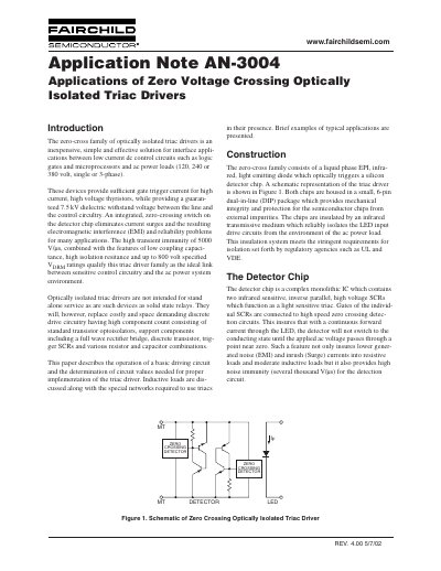
The text details the construction of the device using liquid phase EPI infrared LEDs and silicon detector chips in a 6-pin DIP package. It explains the operation of the detector chip containing high-voltage SCRs that function as a light-sensitive triac, ensuring switching occurs near zero voltage to reduce noise. The note also covers basic driving circuits, resistor calculations for current limiting, and considerations for inductive loads using snubber networks.
The maximum guaranteed current necessary to latch the MOC3061 is 15 mA.
The minimum forward blocking voltage between MT1 and MT2 is 600 volts.
The switch provides a minimum dV/dt of 500 V/s even at an ambient temperature of 70°C.