
TMS320F2810 and TMS320F2812 are digital signal processors that feature high-performance static CMOS technology, high-performance CPU, on-chip memory, external interface, and motor control peripherals.
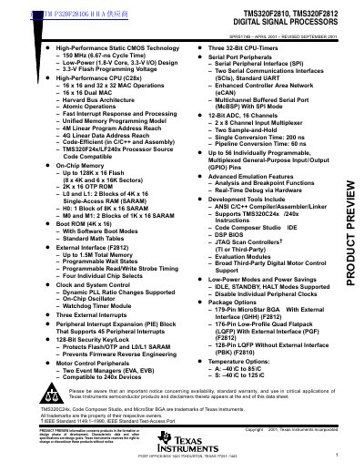
This document is a product preview datasheet for the TMS320F2810 and TMS320F2812 Digital Signal Processors (DSPs). These devices utilize High-Performance Static CMOS Technology with a 150 MHz clock speed, offering low-power operation at 1.8-V core voltage and 3.3-V I/O levels.
The processors feature the C28x CPU architecture with Harvard Bus Architecture, supporting up to 4M linear program address reach and 4G linear data address reach. Key features include on-chip memory options ranging from 64K to 128K of Flash (depending on model), Boot ROM, OTP ROM, and various SARAM blocks. The devices are designed for motor control applications with dedicated Event Managers (EVA, EVB) and support broad third-party digital motor control.
| Instruction Cycle Time | 6.67 ns (at 150 MHz) |
|---|---|
| Core Voltage | 1.8-V |
| I/O Voltage | 3.3-V |
| ADC Resolution | 12-Bit |
| ADC Conversion Time (Single) | 200 ns |
| ADC Conversion Time (Pipeline) | 60 ns |
| GPIO Pins | Up to 56 |
The F2812 includes an External Interface for up to 1.5M total memory, while the F2810 does not have this interface.
The F2810 is available in a 128-pin LQFP without external interface, while the F2812 offers 179-Pin MicroStar BGA and 176-Pin Low-Profile Quad Flatpack.
Yes, it is fully compatible with TMS320C24x/LF240x Processor Source Code.