
ADN2819 is a multirate to 2.7 Gb/s clock and data recovery IC with integrated limiting amp produced by Analog Devices, with excellent performance.
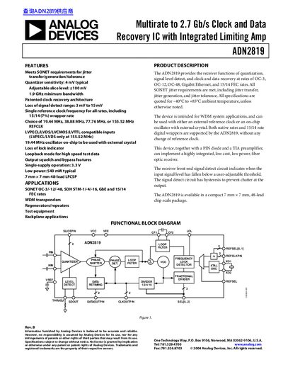
The ADN2819 is an integrated circuit designed for receiver functions including quantization, signal level detection, and clock and data recovery. It supports various data rates such as OC-3, OC-12, OC-48, Gigabit Ethernet, and 15/14 FEC rates while meeting SONET jitter requirements.
The device operates on a single supply of 3.3 V with low power consumption (typical 540 mW) and is available in a compact 7 mm x 7 mm 48-lead LFCSP package. It features an on-chip oscillator, loopback mode for testing, and compatibility with LVPECL, LVDS, LVCMOS, and LVTTL inputs.
| Quantizer Sensitivity | 4 mV typical |
|---|---|
| Upper -3 dB Bandwidth | 1.9 GHz |
| Supply Voltage | 3.0 V to 3.6 V |
| Package Type | 7 mm x 7 mm 48-lead LFCSP |
| Operating Temperature Range | -40°C to +85°C |
No, the device can use either an external reference clock or an on-chip oscillator with an external crystal.
The typical low power consumption is 540 mW.