
This document describes the technical data of a low power CMOS complete DDS technology, which has a power supply of +2.5 V to +5.5 V, a speed of 25 MHz, a tiny 10-pin µµµµµSOIC package, serial loading sinusoidal/triangular DAC output, power-down option, narrowband SFDR > 72 dB, and 20 mW power consumption at 3 V.
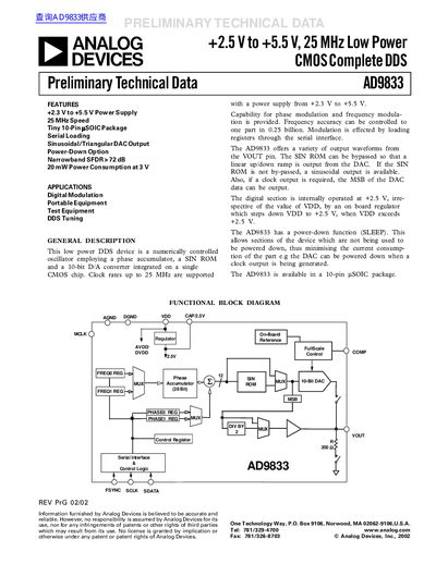
The document describes the AD9833, a numerically controlled oscillator employing a phase accumulator, a SIN ROM, and a 10-bit D/A converter integrated on a single CMOS chip. It supports clock rates up to 25 MHz and offers output waveforms including sinusoidal signals and linear up/down ramps.
| Power Supply Range | +2.3 V to +5.5 V |
|---|---|
| Maximum Clock Rate | 25 MHz |
| DAC Resolution | 10 Bits |
| Update Rate | 25 MSPS |
| Spurious Free Dynamic Range (Narrow Band) | 72 dBc |
| Power Consumption (3V) | 20 mW |
The device supports clock rates up to 25 MHz.
The AD9833 supports clock rates up to 25 MHz.
Current consumption drops to 0.25 mA when the DAC and internal clock are powered down.
The MCLK period must be at least 40 ns to meet timing requirements.