
The content of this document is copyrighted by its respective manufacturer. Unable to provide a summary of the features and characteristics of the products.
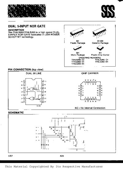
The document describes a high‑speed dual 5‑input NOR gate fabricated in low‑power Schottky technology. It lists ordering numbers (T54LS260, T74LS260) and provides the pin‑connection diagram for the dual in‑line chip carrier package.
Electrical specifications include absolute maximum ratings, guaranteed operating ranges, and detailed DC and AC characteristics such as input/output voltage levels, current limits, and timing parameters.
| Supply Voltage (absolute max) | -0.5 to 7 V |
|---|---|
| Input Voltage (absolute max) | -0.5 to 16 V |
| Output Voltage (absolute max) | -0.5 to 10 V |
| Input Current (absolute max) | -30 to 5 mA |
| Output Current (absolute max) | 50 mA |
| Supply Voltage (guaranteed, T54LS260D02) | 4.5 V min – 5.5 V max (typ 5.0 V) |
| Operating Temperature (guaranteed, T54LS260D02) | -55 °C to +125 °C |
| Input HIGH Voltage (DC characteristic) | ≥ 2.0 V |
| Input LOW Voltage (DC characteristic) | ≤ 0.7 V |
| Output HIGH Voltage (DC characteristic) | Typ 2.5 V, Max 3.4 V |
| Output LOW Voltage (DC characteristic) | Typ 0.25 V, Max 0.4 V |
| Supply Current HIGH (DC characteristic) | Typical 4.0 mA |
| Supply Current LOW (DC characteristic) | Typical 6.5 mA |
The device can tolerate a supply voltage from –0.5 V up to 7 V.
For the T54LS260D02 package the supply voltage is guaranteed between 4.5 V minimum and 5.5 V maximum, with a typical value of 5.0 V.
Each output can source or sink up to 50 mA.
The absolute maximum input voltage range is –0.5 V to 16 V.