
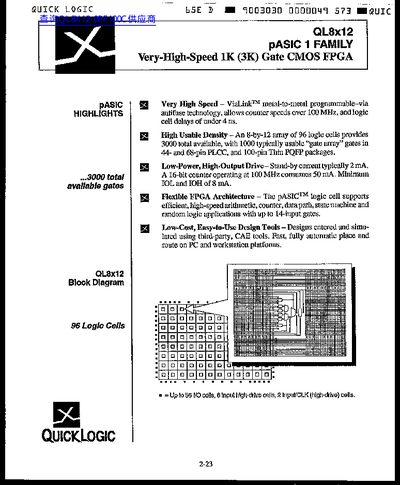
The QL8x12 is a member of QuickLogic's pASIC 1 family, offering a very‑high‑speed CMOS FPGA with 96 logic cells and up to 3000 total gates. It features metal‑to‑metal ViaLink programmable‑via technology, low standby current, and flexible architecture supporting up to 14‑input gates.
The document includes detailed electrical characteristics, pinout information, timing parameters, and absolute maximum ratings, enabling designers to evaluate the device for high‑performance applications such as fast microprocessor interfaces and custom logic implementations.
| Logic cells | 96 |
|---|---|
| Total available gates | 3000 |
| Typical usable gates | 1000 |
| Input HIGH voltage (VIH) | 2.0 V |
| Input LOW voltage (VIL) | 0.8 V |
| Clock‑to‑Q delay (fanout 1) | 3.0 ns |
The QL8x12 contains 96 logic cells.
Chip‑to‑chip operating frequencies can reach up to 85 MHz, with internal state‑machine frequencies up to 100 MHz.