
This data sheet introduces the features of QL4016 QuickRAM ESP, including high performance, high density, high speed embedded SRAM, easy to use and fast development cycle.
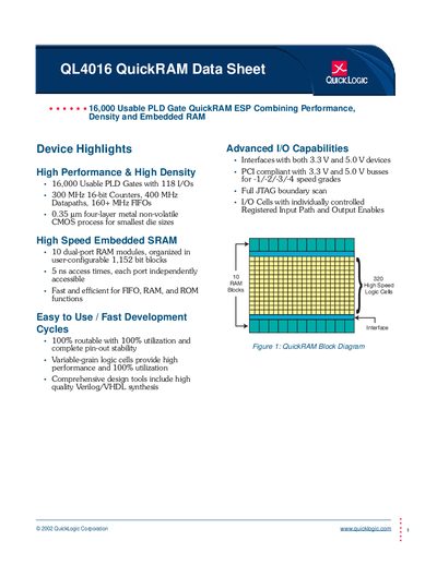
The QL4016 QuickRAM is a 0.35 µm four‑layer metal ESP offering 16 000 usable PLD gates, 320 logic cells and 10 dual‑port RAM modules (1 152 bits each). It supports both 3.3 V and 5.0 V I/O, PCI‑compliant buses and full JTAG boundary‑scan.
Key performance figures include up to 400 MHz datapaths, 300 MHz counters, 160 MHz+ FIFOs and 5 ns access times. The device is available in 84‑pin PLCC, 100‑pin TQFP, 100‑pin CQFP and 144‑pin TOQFP packages, with a supply voltage range of 3.0‑3.6 V and an operating temperature range of –55 °C to +85 °C.
| Usable PLD Gates | 16,000 |
|---|---|
| I/O Pins | 118 |
| Logic Cells | 320 |
| Dual‑Port RAM Modules | 10 |
| RAM Bits per Module | 1,152 |
| Maximum Datapath Speed | 400 MHz |
| Access Time | 5 ns |
| Supply Voltage Range | 3.0 V – 3.6 V |
The QL4016 provides a total of 118 I/O pins.
The device supports datapaths up to 400 MHz.
The embedded RAM has an access time of 5 ns per port.
The QL4016 contains 16 000 usable PLD gates.