
The AD6642 Rev. A is a dual IF receiver with high performance and low power consumption. It features an 11-bit, 200 MSPS output data rate per channel and an integrated noise shaping requantizer (NSR) for high signal-to-noise ratio (SNR) and low distortion. Additionally, it has low power consumption, adjustable analog input range, and various power-down modes.
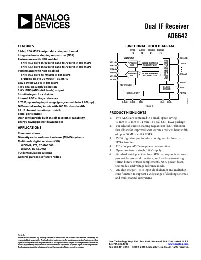
The AD6642 dual‑channel intermediate‑frequency receiver integrates two high‑performance ADCs and a noise‑shaping requantizer (NSR). It delivers 11‑bit resolution at up to 200 MSPS per channel, operates from a single 1.8 V supply, and provides LVDS digital outputs compatible with low‑cost FPGA families.
Designed for telecommunications, MIMO, software‑defined radio and other high‑speed digital‑receiver applications, the device includes SPI control, built‑in self‑test, power‑down modes and extensive design‑guideline recommendations to optimise performance and power consumption.
| Resolution | 11 Bits |
|---|---|
| Output data rate per channel | 200 MSPS |
| Supply voltage (AVDD / DRVDD) | 1.8 V |
| Power consumption (typical) | 0.62 W @ 185 MSPS |
| Analog input range | 1.75 V p‑p differential |
| LVDS output voltage | 247–454 mV |
| Operating temperature range | -40 °C to +85 °C |
The AD6642 can sample at up to 200 MSPS per channel, with typical operation at 185 MSPS.
Both the analog and digital sections run from a 1.8 V supply (AVDD and DRVDD).
The device offers standby and power‑down modes; standby power is 83 mW and power‑down power is 18 mW.