
PhaseLink’s Analog Frequency MultiplierTM (AFM) is the industry’s first ‘Balanced Oscillator’ utilizing analog multiplication of the fundamental frequency (at double or quadruple frequency), combined with an attenuation of the fundamental of the reference crystal, without the use of a phase-locked loop (PLL), in CMOS technology. PhaseLink’s patent pending PL560-xx family of AFM products can achieve up to 800 MHz output frequency with little jitter or phase noise deterioration. In addition, the low frequency input crystal requirement makes the AFMs the most affordable high-performance timing-source in the market. PL560-xx family of products utilize low-power CMOS technology and are housed in GREEN/ RoHS compliant 16-pin TSSOP, and 16-pin 3x3 QFN packages.
The PhaseLink PL560-xx VCXO family provides non‑PLL analog frequency multiplication from 30 MHz up to 200 MHz input, delivering output frequencies between 60 MHz and 800 MHz with ultra‑low jitter and phase noise. The devices are offered in RoHS‑compliant 16‑pin TSSOP and 3 × 3 mm QFN packages and support differential PECL, LVDS or single‑ended CMOS outputs.
The document includes product features, block diagrams, selection guides, crystal and board‑layout recommendations, voltage‑control specifications, external component values, package dimensions and ordering codes. It also describes the tuning assistant software for optimizing inductors and capacitors in custom layouts.
| Input frequency range | 30‑200 MHz |
|---|---|
| Output frequency range | 60‑800 MHz |
| RMS phase jitter | < 0.25 ps (12 kHz‑20 MHz) |
| RMS period jitter | < 2.5 ps |
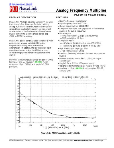
| Phase noise at 100 kHz offset | -142 dBc/Hz (155.52 MHz carrier) |
| Pullability | ±120 ppm |
| Supply voltage | 2.5 V or 3.3 V ±10 % |
| Operating temperature range | -40 °C to +85 °C (optional industrial) |
| Package types | 16‑pin TSSOP, 16‑pin 3 × 3 mm QFN |
The PL560-xx VCXO family accepts input frequencies from 30 MHz to 200 MHz.
They can generate output frequencies up to 800 MHz.
RMS phase jitter is less than 0.25 ps over the 12 kHz‑20 MHz range.
The devices are offered in RoHS‑compliant 16‑pin TSSOP and 16‑pin 3 × 3 mm QFN packages.