
The ADS7826/27/29 is a family of 10/8/12-bit sampling (2.7 V VCC) analog-to-digital converters (A/D) with assured specifications at 2.7-V supply voltage. It requires very little power even when operating at the full sample rate. At lower conversion rates, the high speed of the device enables it to spend most of its time in the power down mode—the power dissipation is less than 60 µW at 75 kHz. The ADS7826/27/29 also features operation from 2.0 V to 5 V, a synchronous serial interface, and a differential input. The reference voltage can be set to any level within the range of 50 mV to VCC.
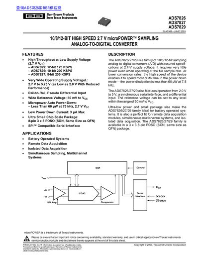
The ADS7826/ADS7827/ADS7829 family provides 10‑bit, 8‑bit and 12‑bit sampling ADCs with high throughput at a low 2.7 V supply. They feature rail‑to‑rail pseudo‑differential inputs, a wide reference voltage range, and ultra‑low power consumption, making them ideal for battery‑operated and remote data‑acquisition systems.
The devices are offered in an 8‑pin 3 × 3 mm SON (PDSO) package and support a SPI‑compatible serial interface. Detailed specifications, pin descriptions, mechanical drawings, and absolute maximum ratings are provided throughout the document.
| Resolution | 12‑bit (ADS7829), 10‑bit (ADS7826), 8‑bit (ADS7827) |
|---|---|
| Maximum Sampling Rate | 125 ksps (ADS7829), 200 ksps (ADS7826), 250 ksps (ADS7827) |
| Power‑Down Current | 3 pA max (typical) |
| Package | 8‑pin 3 × 3 mm SON (PDSO) – same size as QFN |
The ADS7829 can sample at up to 125 ksps.
In power‑down mode the current is less than 3 pA, resulting in sub‑nanowatt power consumption.
They are supplied in an 8‑pin 3 × 3 mm SON (PDSO) package, the same size as a QFN.