
The LTC1282 is a 12-bit A/D converter with a sampling rate of 140ksps and is powered by a single supply with a power consumption of 12mW. It has a built-in 1.14µs sample and hold, a high-precision reference voltage and an internal calibrated clock. It supports single-ended and bipolar conversion modes. The device is built with LTBiCMOS TM switched capacitor technology. It has a 25ppm/°C (max) internal reference voltage, which converts 0V to 2.5V single-ended inputs from a single 3V supply. With ±3V supplies, the input range is ±1.25V with two's complement output format. The maximum DC specifications include ±0.5LSB INL, ±0.75LSB DNL, and 25ppm/°C full-scale drift over temperature. Outstanding AC performance includes 69dB S/(N + D) and 77dB THD at the Nyquist input frequency of 70kHz. The internal clock is trimmed for a maximum conversion time of 6µs. The clock automatically synchronizes to each sample command, eliminating problems with asynchronous clock noise found in competitive devices. A high-speed parallel interface simplifies connections to FIFOs, DSPs, and microprocessors.
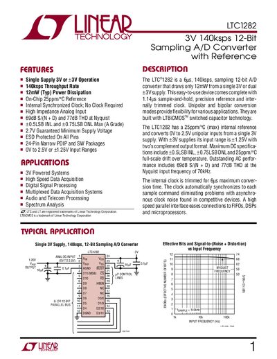
The LTC1282 is a 12‑bit, 140 ksps sampling A/D converter that operates from a single 3 V supply (or dual +3 V). It features an on‑chip 25 ppm/°C reference, high‑impedance analog input, and a synchronized internal clock that eliminates the need for an external clock source. The device offers 69 dB S/(N+D) and 77 dB THD at the Nyquist frequency, making it suitable for high‑speed data acquisition, audio, telecom processing, and spectrum analysis.
The part is supplied in a 24‑lead narrow‑PDIP or a 24‑lead plastic‑wide SO package. Absolute maximum ratings include 12 V total supply and 500 mW power dissipation. Detailed specifications cover resolution, linearity, input ranges, digital I/O characteristics, timing parameters, and typical performance curves. Related parts and ordering information are provided at the end of the document.
| Typical Power Dissipation | 12 mW |
|---|---|
| Supply Voltage (Typical) | 3 V |
| Unipolar Input Range | 0 V to 2.5 V |
| Signal‑to‑Noise Ratio (Nyquist) | 69 dB |
| Total Harmonic Distortion (Nyquist) | 77 dB |
Typical power dissipation is 12 mW at the rated 140 ksps sampling rate.
The device operates from a single 3 V supply (or dual +3 V supplies).
In unipolar mode the analog input range is 0 V to 2.5 V.