
AD9125 is a dual-channel, 16-bit, 1000 MSPS TxDAC+ digital-to-analog converter. It features a flexible CMOS interface that allows dual-word, word, or byte load. The single-carrier W-CDMA ACLR is 80 dBc at 122.88 MHz IF. It has an adjustable analog output, gain and phase adjustment for sideband suppression, multichip synchronization interface, high-performance low-noise PLL clock multiplier, digital inverse sinc filter, and other features. It is suitable for wireless infrastructure, digital high or low IF synthesis, transmit diversity, wideband communications, and other applications.
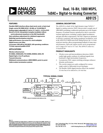
The AD9125 is a dual, 16‑bit, high‑dynamic‑range TxDAC+ digital‑to‑analog converter designed for direct‑conversion transmit applications such as wireless infrastructure and wideband communications. It features a flexible CMOS interface, multichip synchronization, a low‑noise PLL clock multiplier, and programmable output current from 8.7 mA to 31.7 mA.
The datasheet provides detailed specifications, functional block diagrams, pin descriptions, timing validation, and example start‑up sequences. Key performance figures include up to 1000 MSPS sampling, low power consumption (as low as 834 mW in 2× mode), and a wide range of digital interface options.
| Resolution | 16 Bits |
|---|---|
| Maximum Sample Rate | 1000 MSPS |
| Full‑Scale Output Current | 8.66 mA to 31.66 mA |
| Power Consumption (2× mode, PLL off) | 834 mW |
| Maximum Digital Clock Rate | 1000 MHz |
| CMOS Input Logic High Level | 1.2 V |
The AD9125 can sample at up to 1000 MSPS.
The full‑scale output current can be programmed from 8.66 mA to 31.66 mA.
In 2× mode with the PLL off, the device consumes 834 mW.
Logic high is 1.2 V and logic low is 0.6 V.